层次结构设计:
当设计一个结构较复杂的系统时,采用层次化和模块化的设计方法,可以使系统设计变得简洁和方便。层次化设计是分层次、分模块地进行设计描述。
描述器件总功能的模块放在最上层,称为顶层设计;
描述器件某一部分功能的模块放在下层,称为底层设计。
四个例子:
- 计数显示电路
- 可编程并行I/O接口设计
- SCI串行数据传送
- 存储器设计
计数显示电路
输出为3位BCD码的计数显示电路。该计数显示电路由三个模块构成:
- 十进制计数器(BVD_CNT)
- 七段显示译码器电路(DEC_LED)
- 分时总线切换电路(SCAN)
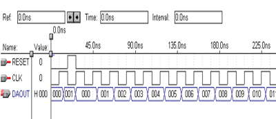
根据逻辑图采用层次化的设计方法,电路原理如图所示:
根据逻辑图采用层次化的设计方法,电路原理如图所示:
(1)顶层模块
library ieee;
use ieee.std_logic_1164.all;
use ieee.std_logic_arith.all;
use ieee.std_logic_unsigned.all;
entity top is
port(clk,reset:in std_logic;
	CL:in std_logic;
	c1,c2,c3:out std_logic_vector(3 downto 0);
	ledout:out std_logic_vector(6 downto 0);
	q:out std_logic_vector(3 downto 0);
	sel:out std_logic_vector(2 downto 0));
end top;

architecture content of top is
signal c1_1,c2_1,c3_1:std_logic_vector(3 downto 0);
signal q_1:std_logic_vector(3 downto 0);
component BCD_CNT is
	port(clk,reset:in std_logic;
		c1,c2,c3:out std_logic_vector(3 downto 0));
end component;
component SCAN is
	port(c1,c2,c3:in std_logic_vector(3 downto 0);
		CL:in std_logic;
		q:out std_logic_vector(3 downto 0);
		sel:out std_logic_vector(2 downto 0));
end component;
component DEC_LED is
	port(q:in std_logic_vector(3 downto 0);
		ledout:out std_logic_vector(6 downto 0));
end component;
begin
u1:BCD_CNT port map(clk,reset,c1_1,c2_1,c3_1);
u2:SCAN port map(c1_1,c2_1,c3_1,CL,q_1,sel);
u3:DEC_LED port map(q_1,ledout);
c1<=c1_1;
c2<=c2_1;
c3<=c3_1;
q<=q_1;
end content;
(2)十进制计数器电路(BCD_CNT)模块:
library ieee;
use ieee.std_logic_1164.all;
use ieee.std_logic_arith.all;
use ieee.std_logic_unsigned.all;

entity BCD_CNT is
	port(clk,reset:in std_logic;
		c1,c2,c3:out std_logic_vector(3 downto 0));
	end BCD_CNT;

architecture cnt of BCD_CNT is
signal cn1,cn2,cn3:std_logic_vector(3 downto 0);
	begin
		cnt1:process(clk,reset)
			begin
				if(reset='1') then cn1<="0000";
				elsif(clk'event and clk='1') then
					if(cn1<9) then cn1<=cn1+1;
					else cn1<="0000";
					end if;
				end if;
			end process cnt1;
			c1<=cn1;
		cnt2:process(cn1(3),reset)
			begin
				if(reset='1') then cn2<="0000";
				elsif(cn1(3)'event and cn1(3)='0') then
					if(cn2<9) then cn2<=cn2+1;
					else cn2<="0000";
					end if;
				end if;
			end process cnt2;
			c2<=cn2;
		cnt3:process(cn2(3),reset)
			begin
				if(reset='1') then cn3<="0000";
				elsif(cn2(3)'event and cn2(3)='0') then
					if(cn3<9) then cn3<=cn3+1;
					else cn3<="0000";
					end if;
				end if;
			end process cnt3;
			c3<=cn3;
end cnt;
(3)分时总线切换电路(SCAN)模块
library ieee;
use ieee.std_logic_1164.all;
use ieee.std_logic_arith.all;
use ieee.std_logic_unsigned.all;

entity SCAN is
	port(c1,c2,c3:in std_logic_vector(3 downto 0);
		cl:in std_logic;
		q:out std_logic_vector(3 downto 0);
		sel:out std_logic_vector(2 downto 0));
end SCAN;

architecture one of SCAN is
signal cnt:std_logic_vector(1 downto 0);
signal q_temp:std_logic_vector(3 downto 0);
signal sel_temp:std_logic_vector(2 downto 0);
begin
	p1:process(cl)
	begin
		if(cl'event and cl='1') then
			if(cnt<2) then cnt<=cnt+1;
			else cnt<="00";
			end if;
		end if;
	end process p1;
	p2:process(cnt)
		begin
			case cnt is
			when "00"=>q_temp<=c1;sel_temp<="001";
			when "01"=>q_temp<=c2;sel_temp<="010";
			when "10"=>q_temp<=c3;sel_temp<="100";
			when others=>null;
		end case;
	end process p2;
	q<=q_temp;
	sel<=sel_temp;
end one;
(4)七段显示译码器电路(DEC_LED)模块
library ieee;
use ieee.std_logic_1164.all;
use ieee.std_logic_arith.all;
use ieee.std_logic_unsigned.all;
entity DEC_LED is
	port(q:in std_logic_vector(3 downto 0);
		ledout:out std_logic_vector(6 downto 0));
end DEC_LED;
architecture one of DEC_LED is
	begin
		process(q)--七段译码电路
			begin
				case q is
				when "0000"=>ledout<="1111110";
				when "0001"=>ledout<="0110000";
				when "0010"=>ledout<="1101101";
				when "0011"=>ledout<="1111001";
				when "0100"=>ledout<="0110011";
				when "0101"=>ledout<="1011011";
				when "0110"=>ledout<="1011111";
				when "0111"=>ledout<="1110000";
				when "1000"=>ledout<="1111111";
				when "1001"=>ledout<="1111011";
				when others=>null;
				end case;
		end process;
end one;
分时总线切换电路仿真结果:将12位二进制数据总线分时送到七段显示译码器电路和芯片外部的译码驱动电路。
十进制计数器仿真结果:十进制计数器(BCD_CNT)完成计数长度为0~999的BCD码加法计数,输出数据总线的宽度为12位。
可编程并行I/O接口设计
以intel 8255为例。
共三种操作模式:
  方式0:基本的输入/输出;
  方式1:有选通的输入/输出;
  方式2:双向总线输入输出。
典型应用:
  8255扩展EPROM编程接口;
  8031单片机使用8255扩展I/O的独立按键。
8255内部结构及信号定义(四部分):
(1)D0–D7: 数据总线缓冲器, 双向;三态;是8255A与CPU系统总线的接口(由数据线与系统总线相接)。
(2)读写控制逻辑:控制总线的开关、信息传输的方向及端口地址选择。与外部连接线:RD、WR、A1、A0、CS和RESET
(3)数据端口:A、B、C三端口;8位(PA0–PA7、PB0–PB7、PC0–PC7);双向;具有输入缓冲、输出锁存。
(4)A组、B组控制电路:A组由A口和C口PC4–PC7组成,B组由B口和C口PC0–PC3组成,内有控制寄存器. 8255的工作方式的设定,就是通过CPU向这三个寄存器写控制字完成的。
8255的基本特性:
8255具有二个8位、二个4位的并行I/O端口的芯片;
8255能以多种形式,在I/O端口与CPU之间进行数据传送。如:程序直接传送、应答方式传送和中断方式传送等。
有4个端口地址:A、B、C三个数据端口地址和控制口地址。一般情况下该芯片的A1、A0脚接系统总线的A1、A0,此时,
A1A0=11时选择的是控制口;
A1A0=00时选择的是A口;
A1A0=01时选择的是B口;
A1A0=10时选择的是C口;
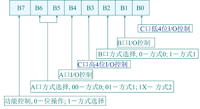
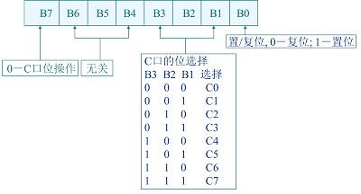
8255的工作方式选择和C口按位操作控制字均利用控制口发布命令。传送数据时用各数据口的地址。
8255有三种工作方式:
方式0:
基本I/O方式。无须连接信号的直接I/O,三个8位口均可作此类I/O。无专用联络信号,不能采用中断方式与CPU交换数据,输出锁存,输入缓冲(有三态门)而无锁存。A口、B口的8条线,C口的高四位和低四位分别对应的4条线均可独立定义,共有16种组合。
方式1:
选通方式。只有A口、B口可作此方式使用,C口此时作为联络线或0方式使用;
方式2:
双向I/O。只有A口可以作为此方式使用,C口在此方式下有5条线作联络线,余下的做B口1方式的联络线。
C口的8位引线,在不同的工作方式下用途不一样,且定义也不相同,使用时要特别小心。
根据功能描述, 8255由锁存器、三态缓冲器、组合逻辑电路构成:

锁存器:7个包括:
  pa_latch--A口输出锁存器,8位;
  pb_latch-- B口输出锁存器,8位;
  pcl_latch-- C口低4位输出锁存器;
  pch_latch-- C口高4位输出锁存器;
  ctrreg--方式控制字寄存器;
  bctrreg--C口位控制字寄存器,4位;
  ctrregF--选择标志寄存器,1位;为'1'时数据存入方式控制字寄存器,为'0'时数据的低四位存入C口控制字寄存器
三态缓冲器,包括:
  数据线D0~D7;
  端口PA、PB、PC;
  以上都是双向的,必须是三态的。
组合逻辑电路:余下部分, 如选择电路、译码电路等。
可编程芯片8255,方式0
LIBRARY IEEE;
USE IEEE.STD_LOGIC_1164.ALL;
USE IEEE.STD_LOGIC_ARITH.ALL;
USE IEEE.STD_LOGIC_UNSIGNED.ALL;
ENTITY ppi IS
   PORT( reset, rd, wr, cs, a0, a1: IN STD_ULOGIC;
            Pa : INOUT STD_ULOGIC_VECTOR(7 DOWNTO 0);
            Pb : INOUT STD_ULOGIC_VECTOR(7 DOWNTO 0);
            Pcl : INOUT STD_ULOGIC_VECTOR(7 DOWNTO 0);
            Pch : INOUT STD_ULOGIC_VECTOR(7 DOWNTO 0);
            d : INOUT STD_ULOGIC_VECTOR(7 DOWNTO 0) );
END ppi;
ARCHITECTURE i8255 OF ppi IS
    signal internal_bus_out : STD_ULOGIC_VECTOR(7 DOWNTO 0);
    signal internal_bus_in : STD_ULOGIC_VECTOR(7 DOWNTO 0);
    signal st, ad, flag : STD_ULOGIC_VECTOR(1 DOWNTO 0);
    signal ctrreg : STD_ULOGIC_VECTOR(7 DOWNTO 0);
    signal pa_lach, pb_lach, pc_lach: STD_ULOGIC_VECTOR(7 DOWNTO 0);
BEGIN
   p1: process(rd, cs)
   p2: process(cs, wr, reset)
   p3: process(pa_latch)
   p4: process(pb_latch)
   p5: process(pc_latch)
   p6: process(pc_latch)
END i8255;
p1: process(rd, cs)   -- 读入进程,
begin
    st <= ctrreg(3) & ctrreg(0);
    if (cs='0' and rd='0') then
       if (a1='0' and a0='0' and ctrreg(4)='1') then
          internal_bus_in <=pa;
       elsif (a1='0' and a0='1' and ctrreg(1)='1') then
          internal_bus_in <=pb;
       elsif (a1='1' and a0='0' and st="01") then
          internal_bus_in(3 downto 0) <=pcl;
       elsif (a1='1' and a0='0' and st="10") then
          internal_bus_in(7 downto 4) <=pch;
       elsif (a1='1' and a0='0' and st="11" and ctrreg(7)='1') then
          internal_bus_in(3 downto 0) <=pcl;
          internal_bus_in(7 downto 4) <=pch;
       end if;
   else
      internal_bus_in <="ZZZZZZZZ";
   end if;
   d <= internal_bus_in ;
end process p1;
p2: process(cs, wr, reset)
    variable ctrregF: std_ulogic;
    variable bctrreg_v: std_ulogic_vector(3 downto 0);
begin
	--用于判断方式控制字还是位控制字
    if (cs='0' and wr='0') then
       ad <= a1 & a0;  ctrregF := d(7); internal_bus_out <= d;
    end if;
    if (reset='1') then
       pa_latch <= "00000000"; pb_latch <= "00000000"; pc_latch <= "00000000";
	   --所有端口均为方式0,输入状态
       ctrreg <= "10011011";
       bctrreg_v := "0000";       ctrregF := '0';
    elsif (wr'event and wr='1') then
       if  (ctrregF='1' and ad="11" and cs='0') then
		--方式控制字时,判断写入的寄存器或锁存器
          ctrreg <= internal_bus_out;
       elsif (ctrreg(7)='1' and ad="00" and cs='0') then
          pa_latch <= internal_bus_out;
       elsif (ctrreg(7)='1' and ad="01" and cs='0') then
          pb_latch <= internal_bus_out;
       elsif (ctrreg(7)='1' and ad="10" and cs='0') then
          pc_latch <= internal_bus_out;
       end if;
       if  (ctrregF='0' and ad="11" and cs='0') then
          bctrreg_v <= internal_bus_out(3 downto 0);
			--位控制字时,对C口各个位的写入
          case bctrreg_v is
              when "0000" =>pc_latch(0)<= '0';
			when "0010" =>pc_latch(1)<= '0';
			when "0100" =>pc_latch(2)<= '0';
			when "0110" =>pc_latch(3)<= '0';
			when "1000" =>pc_latch(4)<= '0';
			when "1010" =>pc_latch(5)<= '0';
			when "1100" =>pc_latch(6)<= '0';
			when "1110" =>pc_latch(7)<= '0';
			when "0001" =>pc_latch(0)<= '1';
			when "0011" =>pc_latch(1)<= '1';
			when "0101" =>pc_latch(2)<= '1';
			when "0111" =>pc_latch(3)<= '1';
			when "1001" =>pc_latch(4)<= '1';
			when "1011" =>pc_latch(5)<= '1';
			when "1101" =>pc_latch(6)<= '1';
			when "1111" =>pc_latch(7)<= '1';
			when others =>flag<= "11";
          end case;
      end if;
   end if;
end process p2;
p3: process(pa_latch)
begin
    if (ctrreg(4)='0' ) then
         pa <= pa_latch;
    else
         pa <= "ZZZZZZZZ";
    end if;
end process p3;
p4: process(pb_latch)
begin
    if (ctrreg(1)='0' ) then
         pb <= pb_latch;
    else
         pb <= "ZZZZZZZZ";
    end if;
end process p4;
p5: process(pc_latch)
begin
    if (ctrreg(0)='0' ) then
         pcl <= pc_latch(3 downto 0);
    else
         pcl <= "ZZZZ";
    end if;
end process p5;
p6: process(pc_latch)
begin
    if (ctrreg(3)='0' ) then
         pch <= pc_latch(7 downto 4);
    else
         pch <= "ZZZZ";
       end if;
end process p6;
SCI串行数据传送
(1)引脚图
共20个,其中17个是有效的输入输出信号引脚。
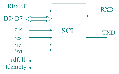
(2)内部结构:功能和性能固定,非程序可编。
(3)串行数据传送格式:传送一个数据或一个字符共需10位。1个启动位(0),8个数据位,一个停止位(1)。每个数据包含4个时钟周期。
(4)串行数据传送的控制机构:
接收同步控制:由6位计数器控制(高4位,低2位)
发送同步控制:由信号tdempty(0)启动
LIBRARY IEEE;
USE IEEE.STD_LOGIC_1164.ALL;
USE IEEE.STD_LOGIC_ARITH.ALL;
USE IEEE.STD_LOGIC_UNSIGNED.ALL;
ENTITY sci IS
   PORT(clk, reset, rxd, rd, wr, cs: IN STD_ULOGIC;
              txd, rdfull, tdempty : OUT STD_ULOGIC;
              data : INOUT STD_LOGIC_VECTOR(7 DOWNTO 0));
END sci;
ARCHITECTURE rtl OF sci IS
    signal scir: STD_ULOGIC_VECTOR(5 DOWNTO 0);  -- 接收计数器
    signal scit: STD_ULOGIC_VECTOR(5 DOWNTO 0);  -- 发送计数器
    signal sh_r: STD_ULOGIC_VECTOR(3 DOWNTO 0);
    signal sl_r: STD_ULOGIC_VECTOR(1 DOWNTO 0);
    signal sh_t: STD_ULOGIC_VECTOR(3 DOWNTO 0);
    signal sl_t: STD_ULOGIC_VECTOR(1 DOWNTO 0);
    signal d_fb: STD_ULOGIC_VECTOR(7 DOWNTO 0); -- 移位寄存器
    signal din_latch: STD_ULOGIC_VECTOR(7 DOWNTO 0);
    signal do_latch: STD_ULOGIC_VECTOR(7 DOWNTO 0);
    signal txdF, rxdF: STD_ULOGIC;  -- 发送和接收的中间标志
    signal tdempty_s: STD_ULOGIC := '1'; -- 发送完毕的标志
    signal rdfull_s: STD_ULOGIC := '0';  -- 接收满的标志
BEGIN
   sh_r<=scir(5 downto 2);
   sl_r <=scir(1 downto 0);
   sh_t<=scit(5 downto 2);
   sl_r <=scir(1 downto 0);
   tdempty<=tdempty_s;
   rdfull<=rdfull_s;
process(clk, rd, cs)    --- 1
BEGIN
   if (rd='0' and cs='0') then  -- 即读数据状态
      rdfull_s<='0';  -- 标记数据已读完;
   elsif (clk'event and clk='1') then
      if (rxdF='1' and sh_r="1111" and sl_r="11") then
          do_latch <= d_fb;
          rdfull_s<='1'; --  data ready,通知CPU发出rd信号
      end if;
   end if;
end process;
--"读"有关进程:  对rdfull进行标记:
--'0'  -- 数据已读完,为下一次读做准备;
--'1'; -- 数据已在锁存器中准备好,可以读取;

process(clk)   ---  3
BEGIN
   if (clk'event and clk='1') then
      if (rxd='0') then   -- 启动位到达
          rxdF <= '1';
      elsif (rxdF='1' and sh_r="1111" and sl_r="11") then
          rxdF <='0';   -- 8位数据接收完毕
      end if;
   end if;
end process;
--- “读”有关进程:  对rxdF进行标记:
--- '1'  -- 数据正在接收;
--- '0'; -- 数据接受完毕;

process(rd, cs)  --- 5
   variable do_latch_v: STD_ULOGIC_VECTOR(7 DOWNTO 0);
BEGIN
   do_latch_v:=do_latch;
   if (rd='0' and cs='0') then   --  read data from do_latch
      data<=TO_STDLOGICVECTOR(do_latch_v);
   else
      data<="ZZZZZZZZ";
   end if;
end process;
--- “读“有关进程:  读锁存器数据到总线data

process(clk, reset)    ---  6
   variable scir_v: INTEGER RANGE 0 TO 63;
   variable scir_s: STD_LOGIC_VECTOR(5 DOWNTO 0);
BEGIN
   if (reset='0') then
      scir_v:='0'; -- "000000";
   elsif (clk'event and clk='1') then
      if (scir_v<=27 and rxd='0') then    ---scir_v<="011011"且''开始位''到达
          scir_v:=28;        --- scir_v="011100"
      elsif (scir_v<=27 and rxd='1') then ---scir_v<="011011"且为''停止位''
          scir_v:='0';
      else
          scir_v:=scir_v+1;
   end if;
   scir_s:=CONV_STD_LOGIC_VECTOR(scir_v,6);
   scir:=TO_STDULOGICVECTOR(scir_s);
end process;
--- "读"有关进程: 数据接收控制过程,即计数器过程。

process(clk, reset)    ---  8
BEGIN
   if (reset='0') then
      d_fb<="00000000";
   elsif (clk'event and clk='1') then
      if (sh_r>="1000" and sh_r<="1111" and sl_r="01") then
          d_fb(7)<=rxd;
          for i in 0 to 6 loop
              d_fb(i)<=d_fb(i+1);   -- 必须先接收低位数据
          end loop;
      end if;
   end if;
end process;
--- "读"有关进程: 数据接收时的移位控制,即串并变换。

process(wr, cs)   --- 2
   variable data_v: STD_ULOGIC_VECTOR(7 DOWNTO 0);
BEGIN
   if (wr'event and wr='1') then  -- 写一个8位数据
      if (cs='0') then
          data_v :=data;
          din_latch<=TO_STDULOGICVECTOR(data_v);
      end if;
   end if;
end process;
--- "写"有关进程:写数据到锁存器。

process(wr, clk)   ---  4
BEGIN
   if (wr='0' and cs='0') then   -- 写数据到发送寄存器
      txdF<='0'; tdempty_s<='0';  -- 寄存器将得到数据
   elsif (clk'event and clk='1') then
      if ((txdF='0' and sh_t="1111" and sl_t="11") or reset='0') then
          txdF<='1'; tdempty_s<='1';  -- 发送结束
      end if;
   end if;
end process;
--- “写”有关进程:  对txdF和tdempty操作:
--- txdF='0',tdempty='0': 发送数据;
--- txdF='1',tdempty='1': 发送结束;

process(clk, reset)    ---  7
   variable scit_v: INTEGER RANGE 0 TO 63;
   variable scit_s: STD_LOGIC_VECTOR(5 DOWNTO 0);
BEGIN
   if (reset='0') then
      scit_v:='0'; -- "000000";
   elsif (clk'event and clk='1') then
      if (scit_v<=27) then    ---scir_v<="011011"
          if (tdempry_s='0' and wr='1') then   --寄存器中数据未发送
              scit_v:=28;          --- scir_v="011100"
          else
              scit_v:='0';          ---寄存器中数据已发送

          end if;
      else         --- 发送下一个数据
          scit_v:=scit_v+1;
      end if;
   end if;
   scit_s:=CONV_STD_LOGIC_VECTOR(scit_v, 6);
   scit:=TO_STDULOGICVECTOR(scit_s);
end process;
--"写"有关进程:  数据发送控制,
--开始计数周期,结束后等待下一个发送数据

process(sh_t)    ---  9
BEGIN
   case sh_t IS
      when "0111"=>txd<='0';
      when "1000"=>txd<=din_latch(0); -- 先发送低位数据
      when "1001"=>txd<=din_latch(1);
      when "1010"=>txd<=din_latch(2);
      when "1011"=>txd<=din_latch(3);
      when "1100"=>txd<=din_latch(4);
      when "1101"=>txd<=din_latch(5);
      when "1110"=>txd<=din_latch(6);
      when "1111"=>txd<=din_latch(7);
      when others=>txd<='1';
   end case;
end process;
end rtl;  ---  end
--"写"有关进程: 数据发送时的并串变换
仿真结果
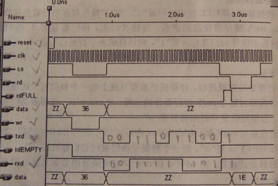
rxd:待接收的数据为”00111 10001”,即1EH
data:待发送的数据为”00110 11001”,即36H
存储器设计
1、数据类型:
(1)存储单元的一个集合体,按单元号顺序排列;
(2)每个单元由若干个二进制位构成,用于表示单元中的数据;
(3)类似于数组;
(4)但每个单元存放的数可用不同的类型来描述;
例1:TYPE memory IS ARRAY (INTEGER RANGE<>) OF INTEGER;
          只存放整数。
例2:SUBTYPE word IS STD_LOGIC_VECTOR( k-1 DOWNTO 0);
          TYPE memory IS ARRAY ( 0 TO 2**w-1) OF word;
其中k表示存储单元中的二进制位数,2**w表示存储器的单元个数;
2、初始化:
用VHDL语言描述ROM时,仿真时要预先将内容读到ROM中;
(1)初始化方法:外部文件的读取,即TEXTIO;
(2)系统加电后,ROM只进行一次初始化;
(3)RAM赋值方法相同;

*变量说明*
VARIABLE startup: BOOLEAN := TRUE;
VARIABLE L: LINE;
VARIABLE j: INTEGER;
VARIABLE rom: memory;
FILE romin: TEXT IS IN "rom24s10.in"

*初始化程序*
IF startup THEN
    FOR j IN rom'RANGE LOOP
           READLINE( romin, L);
           READ( L, rom(j));
    END LOOP;
END IF;
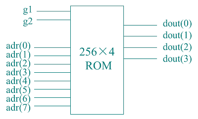
ROM(只读存储器ROM24S10)
容量:256×4
地址线adr(0)~adr(7):用于选中某一单元;
2位选择控制输入g1、g2:g1g2="11"有效;
4位数据输出线dout(0)~dout(3):输出选中单元中的数据;
LIBRARY IEEE;
USE IEEE.STD_LOGIC_1164.ALL;
USE IEEE.STD_LOGIC_UNSIGNED.ALL;
ENTITY rom24s10 IS
   PORT(g1, g2: IN STD_LOGIC;
              adr: IN STD_LOGIC_VECTOR(7 DOWNTO 0);
              dout: OUT STD_LOGIC_VECTOR(3 DOWNTO 0));
END rom24s10;

ARCHITECTURE beh OF rom24s10 IS
       SUBTYPE word IS STD_LOGIC_VECTOR( 3 DOWNTO 0);
TYPE memory IS ARRAY ( 0 TO 255) OF word;
SIGNAL adr_in: INTEGER RANGE 0 TO 255;
FILE romin: TEXT IS IN "rom24s10.in"
BEGIN
       process(g1, g2,adr)
         ---
END beh;
ROM设计:
process(g1, g2,adr)
VARIABLE startup: BOOLEAN := TRUE;
       VARIABLE rom: memory;
       VARIABLE l: LINE;
       VARIABLE j: INTEGER;
begin
IF startup THEN
    FOR j IN rom'RANGE LOOP
           READLINE( romin, l);
           READ( l, rom(j));
    END LOOP;
    startup:= false;
END IF;
adr_in<=CONV_INTEGER(adr);
if (g1='1' and g2='1') then
    dout<=rom(adr_in);
else
    dout<="ZZZZ";
end if;
end process;
RAM(随机存储器)
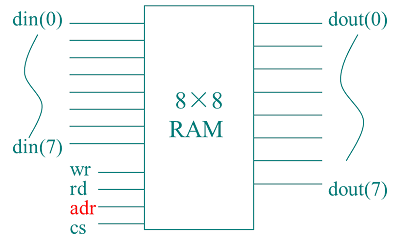
容量:8×8位
地址线adr(0)~adr(2):用于选中某一单元;
8位数据输出线dout(0)~dout(7):输出选中单元中的数据;
8位数据输入线din(0)~din(7):输入选中单元中的数据;
cs
wr
rd

LIBRARY IEEE;
USE IEEE.STD_LOGIC_1164.ALL;
USE IEEE.STD_LOGIC_UNSIGNED.ALL;
ENTITY sram64 IS
   GENERIC(k: INTEGER:=8;
                     w: INTEGER:=3);
   PORT(wr, rd, cs: IN STD_LOGIC;
              adr: IN STD_LOGIC_VECTOR(w-1 DOWNTO 0);
              din: IN STD_LOGIC_VECTOR(k-1 DOWNTO 0));
              dout: OUT STD_LOGIC_VECTOR(k-1 DOWNTO 0));
END sram64;

ARCHITECTURE beh OF rom24s10 IS
       SUBTYPE word IS STD_LOGIC_VECTOR( k-1 DOWNTO 0);
TYPE memory IS ARRAY ( 0 TO 2**w-1) OF word;
SIGNAL adr_in: INTEGER RANGE 0 TO 2**w-1;
SIGNAL sram: memory;
       SIGNAL din_change, wr_rise: time:= 0 ps;
BEGIN
       adr_in<=CONV_INTEGER(adr);
       process(wr)
       process(rd, cs)
---
END beh;
RAM设计:
process(rd, cs)
begin
      if (cs='1' and rd='0')then
dout<=sram(adr_in) after 3 ns;
else
       dout<="ZZZZZZZZ" after 4 ns;
end if;
end process;

process(wr)
begin
if(wr'event and wr='1')then
if (cs='1' and wr='1')then
sram(adr_in)<=din after 2 ns;
end if;
end if;
end process;
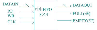
FIFO设计
作为数据缓冲器,数据存放结构和RAM一致;存取方式不同。
4位数据输入线DIN、输出DOUT;
读、写控制;
时钟及两条状态线FULL、EMPTY;
6个功能块:存储体、写指示器(WP)、读指示器(RP)、满逻辑IN_FULL、空逻辑IN_EMPTY、选择逻辑SELECT。
LIBRARY IEEE;
USE IEEE.STD_LOGIC_1164.ALL;
ENTITY fifo IS
   GENERIC(w: INTEGER:=8;
                      k: INTEGER:=4);
   PORT(clk, reset, wr, rd: IN STD_LOGIC;
              din: IN STD_LOGIC_VECTOR(k-1 DOWNTO 0));
              dout: OUT STD_LOGIC_VECTOR(k-1 DOWNTO 0)
              full, empty: OUT STD_LOGIC);
END fifo;

ARCHITECTURE beh OF fifo IS
       SUBTYPE word IS STD_LOGIC_VECTOR( k-1 DOWNTO 0);
TYPE memory IS ARRAY ( 0 TO w-1) OF word;
SIGNAL ram: memory;
       SIGNAL wp, rp: INTEGER RANGE 0 TO w-1;
       SIGNAL in_full, in_empty: STD_LOGIC;
BEGIN
       full<=in_full;
       empty<=in_empty;
       dout<=ram(rp);        --- 数据出栈
       process(clk)             --- 数据进栈
       process(clk, reset)    --- 修改wp
       process(clk, reset)    --- 修改rp
       process(clk, reset)    --- 产生empty标志
       process(clk, reset)    --- 产生full标志
---
END beh;
FIFO设计:
--- 数据进栈
process(clk)
begin
if(clk'event and clk='1')then
if (wr='0' and in_full='0')then
ram(wp)<=din;
end if;
end if;
end process;

--- 修改wp
process(clk, reset)
begin
if (reset=1') then
        wp<=0;
elsif(clk'event and clk='1')then
if (wr='0' and in_full='0')then
if (wp=w-1) then
    wp=0;
elsif
    wp<=wp+1;
end if;
end if;
end if;
end process;

--- 修改rp
process(clk, reset)
begin
if (reset=1') then
        rp<=w-1;
elsif(clk'event and clk='1')then
if (rd='0' and in_empty='0')then
if (rp=w-1) then
    rp=0;
elsif
    rp<=rp+1;
end if;
end if;
end if;
end process;

--- 产生empty标志
process(clk, reset)
begin
if (reset=1') then
        in_empty<='1';
elsif(clk'event and clk='1')then
if ((rd='0' and wr='1') and
   ((rp=wp-2) or (rp=w-1 and wp=1) or (rp=w-2 and wp=0)) then
in_empty='1';
elsif(in_empty='1' and wr='0') then
in_empty<='0';
end if;
end if;
end process;

--- 产生full标志
process(clk, reset)
begin
if (reset=1') then
        in_full<='0';
elsif(clk'event and clk='1')then
if ((rd='1' and wr='0') and (rp=wp)) then
in_full='1';
elsif(in_full='1' and rd='0') then
in_full<='0';
end if;
end if;
end process;
ROM:
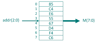
library IEEE;
use IEEE.std_logic_1164.all;
use IEEE.std_logic_unsigned.all;

entity ROM is
    port (
        addr: in STD_LOGIC_VECTOR (2 downto 0);
        M: out STD_LOGIC_VECTOR (7 downto 0)
    );
end ROM;

architecture ROM_arch of ROM is
constant data0: STD_LOGIC_VECTOR (7 downto 0) := "10000101";
constant data1: STD_LOGIC_VECTOR (7 downto 0) := "11000100";
constant data2: STD_LOGIC_VECTOR (7 downto 0) := X"E6";
constant data3: STD_LOGIC_VECTOR (7 downto 0) := X"55";
constant data4: STD_LOGIC_VECTOR (7 downto 0) := X"67";
constant data5: STD_LOGIC_VECTOR (7 downto 0) := X"D4";
constant data6: STD_LOGIC_VECTOR (7 downto 0) := "11110100";
constant data7: STD_LOGIC_VECTOR (7 downto 0) := "11000110";

type rom_array is array (NATURAL range <>) of STD_LOGIC_VECTOR (7 downto 0);
constant rom: rom_array := (
	data0, data1, data2, data3,
	data4, data5, data6, data7
	);
begin
  process(addr)
  variable j: integer;
  begin
    j := conv_integer(addr);
    M <= rom(j);
  end process;
end ROM_arch;